RISC and ARM Architecture
We can gain a basic understanding of the RISC architecture and it’s relation to ARM from the following lines found on ARM’s website.
A Reduced Instruction Set Computer is a type of microprocessor architecture that utilizes a small, highly-optimized set of instructions rather than the highly-specialized set of instructions typically found in other architectures. RISC is an alternative to the Complex Instruction Set Computing (CISC) architecture and is often considered the most efficient CPU architecture technology available today.
ARM, or “Advanced RISC Machine” is a specific family of instruction set architecture that’s based on reduced instruction set architecture developed by Arm Ltd. Processors based on this architecture are common in smartphones, tablets, laptops, gaming consoles and desktops, as well as a growing number of other intelligent devices.
In essence, we can summarize this as:
- RISC - Reduced instruction Set Computer
- CISC - Complex Instruction Set Computer
Important components of a RISC microprocessor are:
- Instructions - Reduced number of instructions
- Pipelines - Instructions are executed in parallel by pipelines
- Registers - Large general-purpose register set
- Load-Store - Processor operates on data held in registers
RISC processors are capable of one instruction per cycle (i.e single cycle processors).
| ARM | Intel x86 | |
|---|---|---|
| Instruction Set | RISC | CISC |
| Endianness | Little, Big endian | Little Endian |
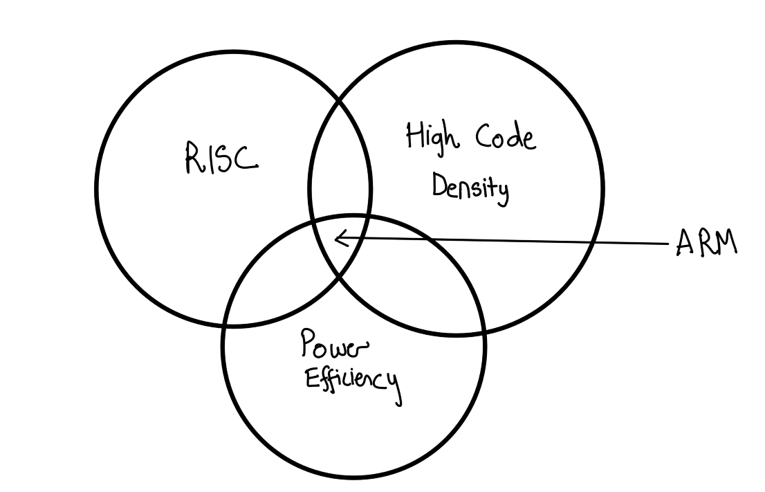
Features of ARM Architecture
ARM architecture derives from the RISC instruction set and are known for being power efficient and having high code density.

Peripherals
ARM Processors are widely used in embedded systems and can be integrated with various peripherals. A peripheral is a part of a microcontroller that interfaces with the outside world and provides it extended functionality and capabilities. Examples of peripherals: GPIO, I2C, SPI, UART, Timers etc.
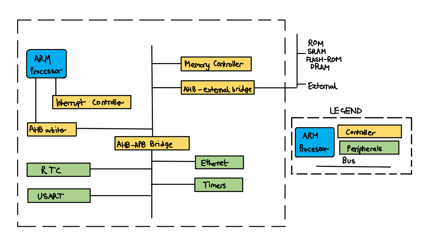
ARM Peripherals are memory mapped.
- Memory Controller: Connects different types of memory to processor
- Interrupt Controller: Determines which peripheral can access the processor at specific times
ARM Bus Technology
Device Classification
Devices on the bus are classified as:
- Bus Master - ARM Processor Core
- Bus Slave - Peripherals
Architecture Levels
There are two bus architecture levels:
-
Physical Level
- Electrical Characteristics
- Bus Width. Ex: 16-bit, 32-bit etc.
-
Protocol Level
- Communication Rules
Types of Bus
- AMBA - Advanced Microcontroller Bus Architecture
- ASB - ARM System Bus
- APB - ARM Peripheral Bus
- AHB - ARM High Performance Bus
Memory
Memory Types
We can again look at the diagram of the ARM processor and its peripherals, to see the various types of memories.
- ROM (Read Only Memory): Cannot be reprogrammed
- Flash ROM: Can be written and read
- DRAM (Dynamic Random Access Memory): Lowest cost per megabyte compared to other RAMs
- SRAM (Static Random Access Memory): Faster than DRAM (does not require pauses between data accesses)
- SDRAM (Synchronous Dynamic Random Access Memory): Runs at much higher clock rate
- EEPROM (Electrically Erasable Programmable Read-Only Memory): Can be written and read. Store critical data that remains intact even when power is off
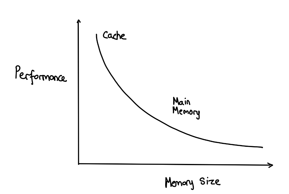
Cache Memory
We have another type of memory known as the cache memory. It is a form of random-access memory that stores recently accessed data and can be used for its quick retrieval. It sits between the main RAM and the CPU, acting as an intermediary for faster data access.
Cache memory is a form of high-speed low-capacity memory. Meanwhile RAM has lower speeds but larger capacities.
Memory Width
It is the number of bits, the memory returns on each access. Ex: 16-bit, 32-bit, 64-bit
| Instruction Size | 8-bit memory | 16-bit memory | 32-bit memory |
|---|---|---|---|
| ARM 32-bit | 4 cycles | 2 cycles | 1 cycle |
| Thumb 16-bit | 2 cycles | 1 cycle | 1 cycle |
Bit Size
32-bit ARM Processors:
- Internal registers in the register bank are 32-bit
- Data paths are 32-bit
- Bus interfaces are 32-bit
Bit size allows the CPU to address memory for an individual process.
xbit can handle2^xbytes of memory
The higher the bit size the higher the performance.
So, 32-bit can handle,
2^32 = 4294967296 bytes ≈ 4.2 GB
Memory Model
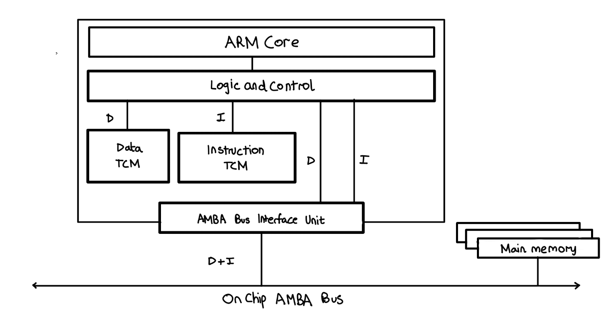
TCM and Cache
Tightly Coupled Memory (TCM) provides low-latency memory accesses that the core can use without the unpredictability of access time that is a feature of caches. When using external, cacheable memory a requested instruction or piece of data might be in the cache, giving a fast access, or might not be in the cache, requiring a slower access to external memory. When using TCM the access time is consistent.
Memory Protection
The allowed configurations for memory protection in ARM microprocessors are:
- No memory protection
- MPU - Memory Protection Unit (simpler)
- MMU - Memory Management Unit (complex)
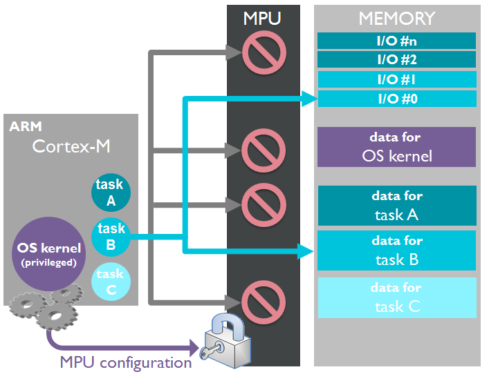
MPU
The MPU is an optional component in Cortex-M processor systems. In systems that require high reliability, the MPU can protect memory regions by defining access permissions for different privilege states. The MPU can also define other memory attributes such as Cacheability, which can be exported to system-level cache unit or memory controllers.
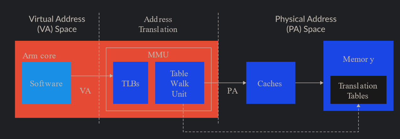
MMU
The Memory Management Unit (MMU) is responsible for the translation of virtual addresses used by software to physical addresses used in the memory system.
The MMU contains the following: - The table walk unit, which contains logic that reads the translation tables from memory. - Translation Lookaside Buffers (TLBs), which cache recently used translations.
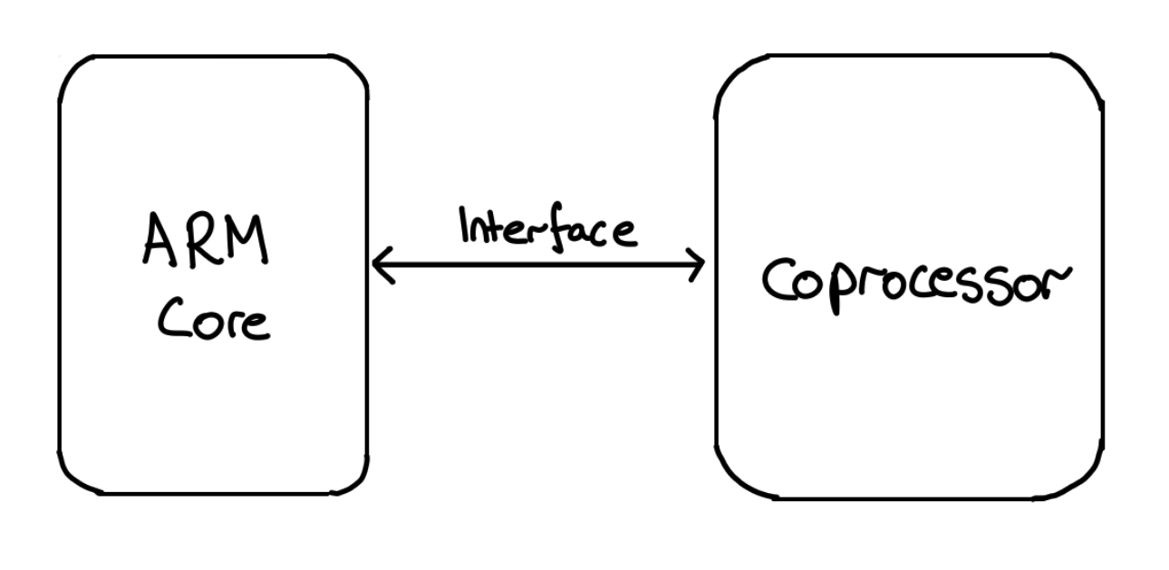
ARM Coprocessors Extension
The processor supports the connection of on-chip coprocessors through an external coprocessor interface. All types of coprocessor instruction are supported.
The ARM instruction set supports the connection of 16 coprocessors, numbered 0-15, to an ARM processor. In the processor, the following coprocessor numbers are reserved:
An example of coprocessors is FPU (Floating Point Unit).